AMD's Radeon HD 5870: Bringing About the Next Generation Of GPUs
by Ryan Smith on September 23, 2009 9:00 AM EST- Posted in
- GPUs
More GDDR5 Technologies: Memory Error Detection & Temperature Compensation
As we previously mentioned, for Cypress AMD’s memory controllers have implemented a greater part of the GDDR5 specification. Beyond gaining the ability to use GDDR5’s power saving abilities, AMD has also been working on implementing features to allow their cards to reach higher memory clock speeds. Chief among these is support for GDDR5’s error detection capabilities.
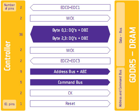
One of the biggest problems in using a high-speed memory device like GDDR5 is that it requires a bus that’s both fast and fairly wide - properties that generally run counter to each other in designing a device bus. A single GDDR5 memory chip on the 5870 needs to connect to a bus that’s 32 bits wide and runs at base speed of 1.2GHz, which requires a bus that can meeting exceedingly precise tolerances. Adding to the challenge is that for a card like the 5870 with a 256-bit total memory bus, eight of these buses will be required, leading to more noise from adjoining buses and less room to work in.
Because of the difficulty in building such a bus, the memory bus has become the weak point for video cards using GDDR5. The GPU’s memory controller can do more and the memory chips themselves can do more, but the bus can’t keep up.
To combat this, GDDR5 memory controllers can perform basic error detection on both reads and writes by implementing a CRC-8 hash function. With this feature enabled, for each 64-bit data burst an 8-bit cyclic redundancy check hash (CRC-8) is transmitted via a set of four dedicated EDC pins. This CRC is then used to check the contents of the data burst, to determine whether any errors were introduced into the data burst during transmission.
The specific CRC function used in GDDR5 can detect 1-bit and 2-bit errors with 100% accuracy, with that accuracy falling with additional erroneous bits. This is due to the fact that the CRC function used can generate collisions, which means that the CRC of an erroneous data burst could match the proper CRC in an unlikely situation. But as the odds decrease for additional errors, the vast majority of errors should be limited to 1-bit and 2-bit errors.
Should an error be found, the GDDR5 controller will request a retransmission of the faulty data burst, and it will keep doing this until the data burst finally goes through correctly. A retransmission request is also used to re-train the GDDR5 link (once again taking advantage of fast link re-training) to correct any potential link problems brought about by changing environmental conditions. Note that this does not involve changing the clock speed of the GDDR5 (i.e. it does not step down in speed); rather it’s merely reinitializing the link. If the errors are due the bus being outright unable to perfectly handle the requested clock speed, errors will continue to happen and be caught. Keep this in mind as it will be important when we get to overclocking.
Finally, we should also note that this error detection scheme is only for detecting bus errors. Errors in the GDDR5 memory modules or errors in the memory controller will not be detected, so it’s still possible to end up with bad data should either of those two devices malfunction. By the same token this is solely a detection scheme, so there are no error correction abilities. The only way to correct a transmission error is to keep trying until the bus gets it right.
Now in spite of the difficulties in building and operating such a high speed bus, error detection is not necessary for its operation. As AMD was quick to point out to us, cards still need to ship defect-free and not produce any errors. Or in other words, the error detection mechanism is a failsafe mechanism rather than a tool specifically to attain higher memory speeds. Memory supplier Qimonda’s own whitepaper on GDDR5 pitches error correction as a necessary precaution due to the increasing amount of code stored in graphics memory, where a failure can lead to a crash rather than just a bad pixel.
In any case, for normal use the ramifications of using GDDR5’s error detection capabilities should be non-existent. In practice, this is going to lead to more stable cards since memory bus errors have been eliminated, but we don’t know to what degree. The full use of the system to retransmit a data burst would itself be a catch-22 after all – it means an error has occurred when it shouldn’t have.
Like the changes to VRM monitoring, the significant ramifications of this will be felt with overclocking. Overclocking attempts that previously would push the bus too hard and lead to errors now will no longer do so, making higher overclocks possible. However this is a bit of an illusion as retransmissions reduce performance. The scenario laid out to us by AMD is that overclockers who have reached the limits of their card’s memory bus will now see the impact of this as a drop in performance due to retransmissions, rather than crashing or graphical corruption. This means assessing an overclock will require monitoring the performance of a card, along with continuing to look for traditional signs as those will still indicate problems in memory chips and the memory controller itself.
Ideally there would be a more absolute and expedient way to check for errors than looking at overall performance, but at this time AMD doesn’t have a way to deliver error notices. Maybe in the future they will?
Wrapping things up, we have previously discussed fast link re-training as a tool to allow AMD to clock down GDDR5 during idle periods, and as part of a failsafe method to be used with error detection. However it also serves as a tool to enable higher memory speeds through its use in temperature compensation.
Once again due to the high speeds of GDDR5, it’s more sensitive to memory chip temperatures than previous memory technologies were. Under normal circumstances this sensitivity would limit memory speeds, as temperature swings would change the performance of the memory chips enough to make it difficult to maintain a stable link with the memory controller. By monitoring the temperature of the chips and re-training the link when there are significant shifts in temperature, higher memory speeds are made possible by preventing link failures.
And while temperature compensation may not sound complex, that doesn’t mean it’s not important. As we have mentioned a few times now, the biggest bottleneck in memory performance is the bus. The memory chips can go faster; it’s the bus that can’t. So anything that can help maintain a link along these fragile buses becomes an important tool in achieving higher memory speeds.


327 Comments
View All Comments
poohbear - Wednesday, September 23, 2009 - link
is it just me or is anyone else disappointed? next gen cards used to double the performance of previous gen cards, this card beats em by a measly 30-40%. *sigh* times change i guess.AznBoi36 - Wednesday, September 23, 2009 - link
It's just you.The next generations never doubled in performance. Rather they offered a bump in framerates (15-40%) along with better texture filtering, AA, AF etc...
I'd rather my games look AMAZING at 60fps rather than crappy graphics at 100fps.
SiliconDoc - Monday, September 28, 2009 - link
Golly, another red rooster lie, they just NEVER stop.Let's take it right from this site, so your whining about it being nv zone or fudzilla or whatever shows ati is a failure in the very terms claimed is not your next, dishonest move.
---
NVIDIA w/ GT200 spanks their prior generation by 60.96% !
That's nearly 61% average increase at HIGHEST RESOLUTION and HIGHEST AA AF settings, and it right here @ AT - LOL -
- and they matched the clock settings JUST TO BE OVERTLY UNFAIR ! ROFLMAO AND NVIDIA'S NEXT GEN LEAP STILL BEAT THE CRAP OUT OF THIS LOUSY ati 5870 EPIC FAIL !
http://www.anandtech.com/video/showdoc.aspx?i=3334...">http://www.anandtech.com/video/showdoc.aspx?i=3334...
--
roflmao - that 426.70/7 = 60.96 % INCREASE FROM THE LAST GEN AT THE SAME SPEEDS, MATCHED FOR MAKING CERTAIN IT WOULD BE AS LOW AS POSSIBLE ! ROFLMAO NICE TRY BUT NVIDIA KICKED BUTT !
---
Sorry, the "usual" is not 15-30% - lol
---
NVIDIA's last usual was !!!!!!!!!!!! 60.69% INCREASE AT HIGHEST SETTINGS !
-
Now, once again, please, no lying.
piroroadkill - Wednesday, September 23, 2009 - link
No, it's definitely just youGriswold - Wednesday, September 23, 2009 - link
Its just you. Go buy a clue.ET - Wednesday, September 23, 2009 - link
Should probably be removed...Nice article. The 5870 doesn't really impress. It's the price of two 4890 cards, so for rendering power that's probably the way to go. I'll be looking forward to the 5850 reviews.
Zingam - Wednesday, September 23, 2009 - link
Good but as seen it doesn't play Crysis once again... :DWe shall wait for 8Gb RAM DDR 7, 16 nm Graphics card to play this damned game!
BoFox - Wednesday, September 23, 2009 - link
Great article!Re: Shader Aliasing nowhere to be found in DX9 games--
Shader aliasing is present all over the Unreal3 engine games (UT3, Bioshock, Batman, R6:Vegas, Mass Effect, etc..). I can imagine where SSAA would be extremely useful in those games.
Also, I cannot help but wonder if SSAA would work in games that use deferred shading instead of allowing MSAA to work (examples: Dead Space, STALKER, Wanted, Bionic Commando, etc..), if ATI would implement brute-force SSAA support in the drivers for those games in particular.
I am amazed at the perfectly circular AF method, but would have liked to see 32x AF in addition. With 32x AF, we'd probably be seeing more of a difference. If we're awed by seeing 16x AA or 24x CFAA, then why not 32x AF also (given that the increase from 8 to 16x AF only costs like 1% performance hit)?
Why did ATI make the card so long? It's even longer than a GTX 295 or a 4870X2. I am completely baffled at this. It only has 8 memory chips, uses a 256-bit bus, unlike a more complex 512-bit bus and 16 chips found on a much, much shorter HD2900XT. There seems to be so much space wasted on the end of the PCB. Perhaps some of the vendors will develop non-reference PCB's that are a couple inches shorter real soon. It could be that ATI rushed out the design (hence the extremely long PCB draft design), or that ATI deliberately did this to allow 3rd-party vendors to make far more attractive designs that will keep us interested in the 5870 right around the time of GT300 release.
Regarding the memory bandwidth bottleneck, I completely agree with you that it certainly seems to be a severe bottleneck (although not too severe that it only performs 33% better than a HD4890). A 5870 has exactly 2x the specifications of a 4890, yet it generally performs slower than a 4870X2, let alone dual-4890 in Xfire. A 4870 is slower than a 4890 to begin with, and is dependent on Crossfire.
Overall, ATI is correct in saying that a 5870 is generally 60% faster than a 4870 in current games, but theoretically, a 5870 should be exactly 100% faster than a 4890. Only if ATI could have used 512-bit memory bandwidth with GDDR5 chips (even if it requires the use of a 1024-bit ringbus) would the total memory bandwidth be doubled. The performance would have been at least as good as two 4890's in crossfire, and also at least as good as a GTX295.
I am guessing that ATI wants to roll out the 5870X2 as soon as possible and realized that doing it with a 512-bit bus would take up too much time/resources/cost, etc.. and that it's better to just beat NV to the punch a few months in advance. Perhaps ATI will do a 5970 card with 512-bit memory a few months after a 5870X2 is released, to give GT300 cards a run for its money? Perhaps it is to "pacify" Nvidia's strategy with its upcoming next-gen that carry great promises with a completely revamped architecture and 512 shaders, so that NV does not see the need to make its GT300 exceed the 5870 by far too much? Then ATI would be able to counter right afterwards without having to resort to making a much bigger chip?
Speculation.. speculation...
Lakku - Wednesday, September 23, 2009 - link
Read some of the other 5780 articles that cover SSAA image quality. It actually makes most modern games look worse, but that is through no fault of ATi, just the nature of the SS method that literally AA's everything, and in the process, can/does blur textures.strikeback03 - Wednesday, September 23, 2009 - link
I don't know much about video games, but in photography it is known that reducing the size of an image reduces the appearance of sharpness as well, so final sharpening should be done at the output size.