AMD's Radeon HD 5870: Bringing About the Next Generation Of GPUs
by Ryan Smith on September 23, 2009 9:00 AM EST- Posted in
- GPUs
Cypress: What’s New
With our refresher out of the way, let’s discuss what’s new in Cypress.
Starting at the SPU level, AMD has added a number of new hardware instructions to the SPUs and sped up the execution of other instruction, both in order to improve performance and to meet the requirements of various APIs. Among these changes are that some dot products have been reduced to single-cycle computation when they were previously multi-cycle affairs. DirectX 11 required operations such as bit count, insert, and extract have also been added. Furthermore denormal numbers have received some much-needed attention, and can now be handled at full speed.
Perhaps the most interesting instruction added however is an instruction for Sum of Absolute Differences (SAD). SAD is an instruction of great importance in video encoding and computer vision due to its use in motion estimation, and on the RV770 the lack of a native instruction requires emulating it in no less than 12 instructions. By adding a native SAD instruction, the time to compute a SAD has been reduced to a single clock cycle, and AMD believes that it will result in a significant (>2x) speedup in video encoding.
The clincher however is that SAD not an instruction that’s part of either DirectX 11 or OpenCL, meaning DirectX programs can’t call for it, and from the perspective of OpenCL it’s an extension. However these APIs leave the hardware open to do what it wants to, so AMD’s compiler can still use the instruction, it just has to know where to use it. By identifying the aforementioned long version of a SAD in code it’s fed, the compiler can replace that code with the native SAD, offering the native SAD speedup to any program in spite of the fact that it can’t directly call the SAD. Cool, isn’t it?
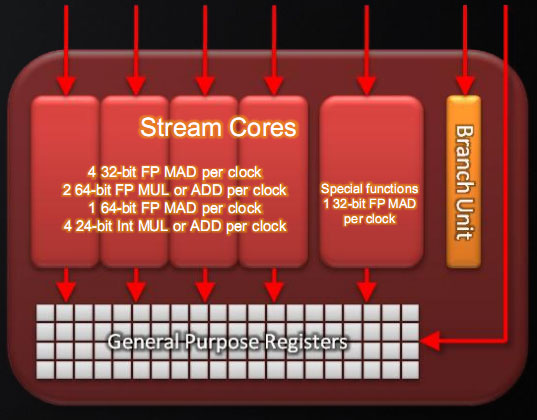
Last, here is a breakdown of what a single Cypress SP can do in a single clock cycle:
- 4 32-bit FP MAD per clock
- 2 64-bit FP MUL or ADD per clock
- 1 64-bit FP MAD per clock
- 4 24-bit Int MUL or ADD per clock
- SFU : 1 32-bit FP MAD per clock
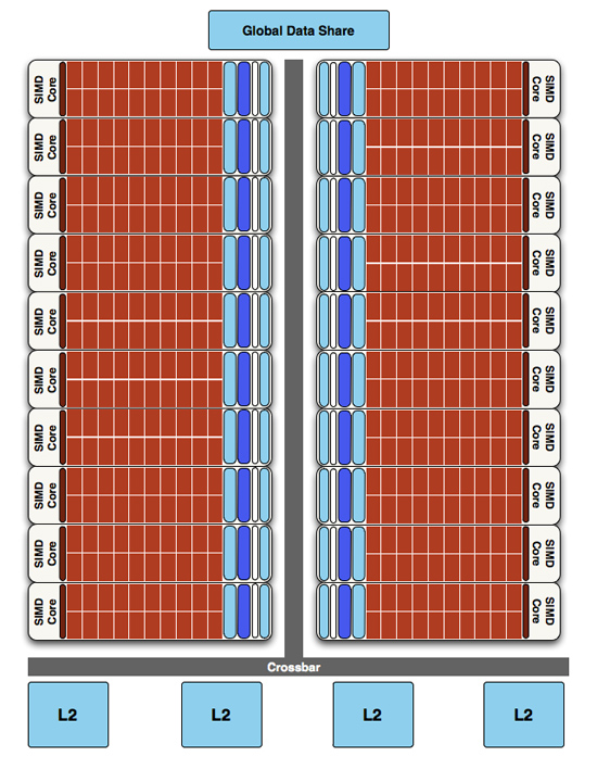
Moving up the hierarchy, the next thing we have is the SIMD. Beyond the improvements in the SPs, the L1 texture cache located here has seen an improvement in speed. It’s now capable of fetching texture data at a blistering 1TB/sec. The actual size of the L1 texture cache has stayed at 16KB. Meanwhile a separate L1 cache has been added to the SIMDs for computational work, this one measuring 8KB. Also improving the computational performance of the SIMDs is the doubling of the local data share attached to each SIMD, which is now 32KB.
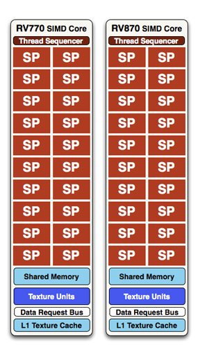
At a high level, the RV770 and Cypress SIMDs look very similar
The texture units located here have also been reworked. The first of these changes are that they can now read compressed AA color buffers, to better make use of the bandwidth they have. The second change to the texture units is to improve their interpolation speed by not doing interpolation. Interpolation has been moved to the SPs (this is part of DX11’s new Pull Model) which is much faster than having the texture unit do the job. The result is that a texture unit Cypress has a greater effective fillrate than one under RV770, and this will show up under synthetic tests in particular where the load-it and forget-it nature of the tests left RV770 interpolation bound. AMD’s specifications call for 68 billion bilinear filtered texels per second, a product of the improved texture units and the improved bandwidth to them.
Finally, if we move up another level, here is where we see the cause of the majority of Cypress’s performance advantage over RV770. AMD has doubled the number of SIMDs, moving from 10 to 20. This means twice the number of SPs and twice the number of texture units; in fact just about every statistic that has doubled between RV770 and Cypress is a result of doubling the SIMDs. It’s simple in concept, but as the SIMDs contain the most important units, it’s quite effective in boosting performance.
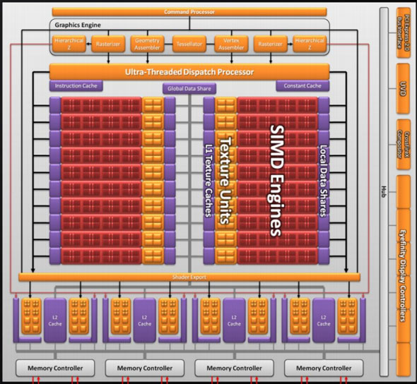
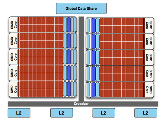
However with twice as many SIMDs, there comes a need to feed these additional SIMDs, and to do something with their products. To achieve this, the 4 L2 caches have been doubled from 64KB to 128KB. These large L2 caches can now feed data to L1 caches at 435GB/sec, up from 384GB/sec in RV770. Along with this the global data share has been quadrupled to 64KB.
RV770 vs...
Cypress
Next up, the ROPs have been doubled in order to meet the needs of processing data from all of those SIMDs. This brings Cypress to 32 ROPs. The ROPs themselves have also been slightly enhanced to improve their performance; they can now perform fast color clears, as it turns out some games were doing this hundreds of times between frames. They are also responsible for handling some aspects of AMD’s re-introduced Supersampling Anti-Aliasing mode, which we will get to later.
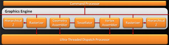
Last, but certainly not least, we have the changes to what AMD calls the “graphics engine”, primarily to bring it into compliance with DX11. RV770’s greatly underutilized tessellator has been upgraded to full DX11 compliance, giving it Hull Shader and Domain Shader capabilities, along with using a newer algorithm to reduce tessellation artifacts. A second rasterizer has also been added, ostensibly to feed the beast that is the 20 SIMDs.


327 Comments
View All Comments
poohbear - Wednesday, September 23, 2009 - link
is it just me or is anyone else disappointed? next gen cards used to double the performance of previous gen cards, this card beats em by a measly 30-40%. *sigh* times change i guess.AznBoi36 - Wednesday, September 23, 2009 - link
It's just you.The next generations never doubled in performance. Rather they offered a bump in framerates (15-40%) along with better texture filtering, AA, AF etc...
I'd rather my games look AMAZING at 60fps rather than crappy graphics at 100fps.
SiliconDoc - Monday, September 28, 2009 - link
Golly, another red rooster lie, they just NEVER stop.Let's take it right from this site, so your whining about it being nv zone or fudzilla or whatever shows ati is a failure in the very terms claimed is not your next, dishonest move.
---
NVIDIA w/ GT200 spanks their prior generation by 60.96% !
That's nearly 61% average increase at HIGHEST RESOLUTION and HIGHEST AA AF settings, and it right here @ AT - LOL -
- and they matched the clock settings JUST TO BE OVERTLY UNFAIR ! ROFLMAO AND NVIDIA'S NEXT GEN LEAP STILL BEAT THE CRAP OUT OF THIS LOUSY ati 5870 EPIC FAIL !
http://www.anandtech.com/video/showdoc.aspx?i=3334...">http://www.anandtech.com/video/showdoc.aspx?i=3334...
--
roflmao - that 426.70/7 = 60.96 % INCREASE FROM THE LAST GEN AT THE SAME SPEEDS, MATCHED FOR MAKING CERTAIN IT WOULD BE AS LOW AS POSSIBLE ! ROFLMAO NICE TRY BUT NVIDIA KICKED BUTT !
---
Sorry, the "usual" is not 15-30% - lol
---
NVIDIA's last usual was !!!!!!!!!!!! 60.69% INCREASE AT HIGHEST SETTINGS !
-
Now, once again, please, no lying.
piroroadkill - Wednesday, September 23, 2009 - link
No, it's definitely just youGriswold - Wednesday, September 23, 2009 - link
Its just you. Go buy a clue.ET - Wednesday, September 23, 2009 - link
Should probably be removed...Nice article. The 5870 doesn't really impress. It's the price of two 4890 cards, so for rendering power that's probably the way to go. I'll be looking forward to the 5850 reviews.
Zingam - Wednesday, September 23, 2009 - link
Good but as seen it doesn't play Crysis once again... :DWe shall wait for 8Gb RAM DDR 7, 16 nm Graphics card to play this damned game!
BoFox - Wednesday, September 23, 2009 - link
Great article!Re: Shader Aliasing nowhere to be found in DX9 games--
Shader aliasing is present all over the Unreal3 engine games (UT3, Bioshock, Batman, R6:Vegas, Mass Effect, etc..). I can imagine where SSAA would be extremely useful in those games.
Also, I cannot help but wonder if SSAA would work in games that use deferred shading instead of allowing MSAA to work (examples: Dead Space, STALKER, Wanted, Bionic Commando, etc..), if ATI would implement brute-force SSAA support in the drivers for those games in particular.
I am amazed at the perfectly circular AF method, but would have liked to see 32x AF in addition. With 32x AF, we'd probably be seeing more of a difference. If we're awed by seeing 16x AA or 24x CFAA, then why not 32x AF also (given that the increase from 8 to 16x AF only costs like 1% performance hit)?
Why did ATI make the card so long? It's even longer than a GTX 295 or a 4870X2. I am completely baffled at this. It only has 8 memory chips, uses a 256-bit bus, unlike a more complex 512-bit bus and 16 chips found on a much, much shorter HD2900XT. There seems to be so much space wasted on the end of the PCB. Perhaps some of the vendors will develop non-reference PCB's that are a couple inches shorter real soon. It could be that ATI rushed out the design (hence the extremely long PCB draft design), or that ATI deliberately did this to allow 3rd-party vendors to make far more attractive designs that will keep us interested in the 5870 right around the time of GT300 release.
Regarding the memory bandwidth bottleneck, I completely agree with you that it certainly seems to be a severe bottleneck (although not too severe that it only performs 33% better than a HD4890). A 5870 has exactly 2x the specifications of a 4890, yet it generally performs slower than a 4870X2, let alone dual-4890 in Xfire. A 4870 is slower than a 4890 to begin with, and is dependent on Crossfire.
Overall, ATI is correct in saying that a 5870 is generally 60% faster than a 4870 in current games, but theoretically, a 5870 should be exactly 100% faster than a 4890. Only if ATI could have used 512-bit memory bandwidth with GDDR5 chips (even if it requires the use of a 1024-bit ringbus) would the total memory bandwidth be doubled. The performance would have been at least as good as two 4890's in crossfire, and also at least as good as a GTX295.
I am guessing that ATI wants to roll out the 5870X2 as soon as possible and realized that doing it with a 512-bit bus would take up too much time/resources/cost, etc.. and that it's better to just beat NV to the punch a few months in advance. Perhaps ATI will do a 5970 card with 512-bit memory a few months after a 5870X2 is released, to give GT300 cards a run for its money? Perhaps it is to "pacify" Nvidia's strategy with its upcoming next-gen that carry great promises with a completely revamped architecture and 512 shaders, so that NV does not see the need to make its GT300 exceed the 5870 by far too much? Then ATI would be able to counter right afterwards without having to resort to making a much bigger chip?
Speculation.. speculation...
Lakku - Wednesday, September 23, 2009 - link
Read some of the other 5780 articles that cover SSAA image quality. It actually makes most modern games look worse, but that is through no fault of ATi, just the nature of the SS method that literally AA's everything, and in the process, can/does blur textures.strikeback03 - Wednesday, September 23, 2009 - link
I don't know much about video games, but in photography it is known that reducing the size of an image reduces the appearance of sharpness as well, so final sharpening should be done at the output size.