AMD's Radeon HD 5870: Bringing About the Next Generation Of GPUs
by Ryan Smith on September 23, 2009 9:00 AM EST- Posted in
- GPUs
A Quick Refresher on the RV770
As Cypress is a direct evolution of the RV770 design, before we talk about what’s new with Cypress we are going to go over a quick rehash of RV770’s internal workings. As it’s necessary to understand how RV770 was built to understand what Cypress changes, if you’re completely unfamiliar with RV770, please take a look at our expanded discussion of RV770 from last year. For the rest of you, let’s get started.
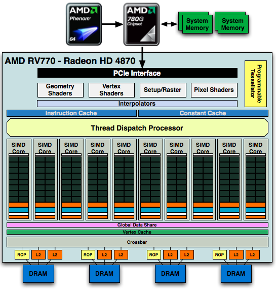
At the center of the RV770 is the Stream Processing Unit (SPU), a single arithmetic logic unit. The RV770 has 800 of these, and they are packaged together in groups of 5 and are what we call a Streaming Processor (SP). A SP contains a register file, a branch predictor, and the aforementioned 5 SPUs, with the 5th SPU being a more complex unit capable of transcendental functions along with the base functions of an ALU. The SP is the smallest unit that can do individual work; every SPU in an SP must execute the same instruction.
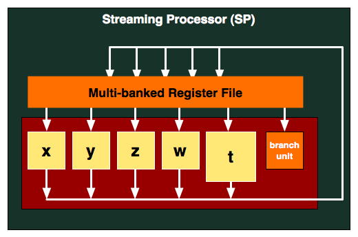
For every 16 SPs, AMD groups them together with texture units, L1 cache, shared memory, and controlling logic. This combined block is what AMD calls a SIMD, and RV770 has 10 of them. These 10 SIMDs form the core computational power of the RV770, and in the chip work with various specialized units such as ROPs, rasterizers, L2 cache, and tesselators to form a complete chip.
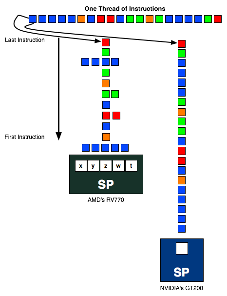
To utilize the computational power of the hardware, instruction threads are issued to the SPs. These threads are grouped into wavefronts, where there are 64 threads per wavefront. To maximize the utilization of the GPU, threads need to be organized so that they can feed all 5 SPUs in a SP an instruction every clock cycle. Doing this requires extracting instruction level parallelism (ILP) out of programs being passed to the GPU, which is difficult task of AMD’s compiler.
If SPUs go unused, then the performance of the chip suffers due to underutilization. This design gives AMD a great deal of theoretical computational power, but it is always a challenge to fully exploit it.


327 Comments
View All Comments
BoFox - Friday, November 6, 2009 - link
Yep, that's turning up LOD to -1 or -2 depending on which game. It was done in Crysis, and with LOD at -2, it looked sharp with SSAA.The Wasrad - Wednesday, September 23, 2009 - link
Why are you using 4 gigs of ram with a 920?Do you understand how DDR3 memory works?
Ryan Smith - Wednesday, September 23, 2009 - link
Error when writing the chart. It has been corrected.Sc4freak - Wednesday, September 23, 2009 - link
Do you? The fact that the i7 920 works best in a triple-channel configuration has nothing to do with the fact that it uses DDR3.chizow - Wednesday, September 23, 2009 - link
Agreed and to add to that, the fact the third channel means very little when it comes to actual gaming performance makes it even less signficant. As compared to Lynnfield clock for clock, which is only dual channel:http://www.anandtech.com/cpuchipsets/showdoc.aspx?...">http://www.anandtech.com/cpuchipsets/showdoc.aspx?...
Von Matrices - Wednesday, September 23, 2009 - link
Could someone enlighten me as to why the 4870 X2 could be faster than the 5870 in some situations? It was noted it the article but never really explained. They have the same number of SP's, and one would expect crossfire scaling to be detrimental to the 4870 X2"s performance. Would this be indicative of the 5870 being starved for memory bandwidth in these situations or something else?Dobs - Wednesday, September 23, 2009 - link
4870x2 has 2Gb of DDR55870 only has 1 until the 2Gb edition comes out :)
nafhan - Wednesday, September 23, 2009 - link
Doesn't using dual GPU's effectively halve the onboard memory, as significant portions of the textures, etc. need to be duplicated? So, the 4870x2 has a memory disadvantage by requiring 2x memory to accomplish the same thing.chizow - Wednesday, September 23, 2009 - link
Right, with an X2 each GPU has a copy of the same frame buffer, so the total memory onboard is effectively halved. A 2GB frame buffer with 2 GPU is two of the same 1GB frame buffer mirrored on each.With the 5870 essentially being 2xRV790 on one chip, in order to accomplish the same frame rates on the same sized 1GB frame buffer, you would expect to need additional bandwidth to facilitate the transfers to and from the frame buffer and GPU.
chizow - Wednesday, September 23, 2009 - link
Ya he mentions bandwidth being a potential issue preventing the 5870 from mirroring the 4870X2's results.It could also be that the 5870's scheduler/dispatch processor aren't as efficient at extracting performance as driver forced AFR. Seems pretty incredible, seeing as physically doubling GPU transistors on a single die has always been traditionally better than multi-GPU scaling.
Similarly, it could be a CPU limitation where CF/SLI benefit more from multi-threaded driver performance, whereas a single GPU would be limited to a single fast thread or core's performance. We saw this a bit as well last year with the GT200s compared to G92s in SLI.