AMD's Radeon HD 5870: Bringing About the Next Generation Of GPUs
by Ryan Smith on September 23, 2009 9:00 AM EST- Posted in
- GPUs
Cypress: What’s New
With our refresher out of the way, let’s discuss what’s new in Cypress.
Starting at the SPU level, AMD has added a number of new hardware instructions to the SPUs and sped up the execution of other instruction, both in order to improve performance and to meet the requirements of various APIs. Among these changes are that some dot products have been reduced to single-cycle computation when they were previously multi-cycle affairs. DirectX 11 required operations such as bit count, insert, and extract have also been added. Furthermore denormal numbers have received some much-needed attention, and can now be handled at full speed.
Perhaps the most interesting instruction added however is an instruction for Sum of Absolute Differences (SAD). SAD is an instruction of great importance in video encoding and computer vision due to its use in motion estimation, and on the RV770 the lack of a native instruction requires emulating it in no less than 12 instructions. By adding a native SAD instruction, the time to compute a SAD has been reduced to a single clock cycle, and AMD believes that it will result in a significant (>2x) speedup in video encoding.
The clincher however is that SAD not an instruction that’s part of either DirectX 11 or OpenCL, meaning DirectX programs can’t call for it, and from the perspective of OpenCL it’s an extension. However these APIs leave the hardware open to do what it wants to, so AMD’s compiler can still use the instruction, it just has to know where to use it. By identifying the aforementioned long version of a SAD in code it’s fed, the compiler can replace that code with the native SAD, offering the native SAD speedup to any program in spite of the fact that it can’t directly call the SAD. Cool, isn’t it?
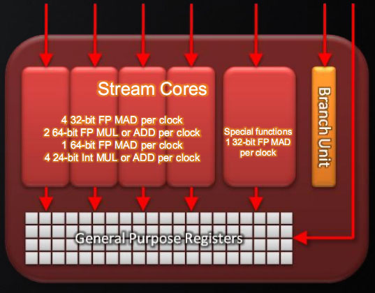
Last, here is a breakdown of what a single Cypress SP can do in a single clock cycle:
- 4 32-bit FP MAD per clock
- 2 64-bit FP MUL or ADD per clock
- 1 64-bit FP MAD per clock
- 4 24-bit Int MUL or ADD per clock
- SFU : 1 32-bit FP MAD per clock
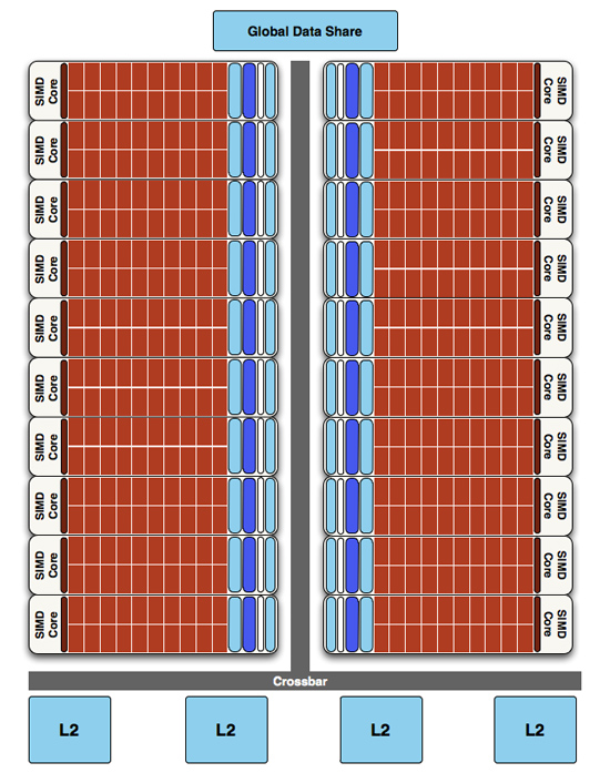
Moving up the hierarchy, the next thing we have is the SIMD. Beyond the improvements in the SPs, the L1 texture cache located here has seen an improvement in speed. It’s now capable of fetching texture data at a blistering 1TB/sec. The actual size of the L1 texture cache has stayed at 16KB. Meanwhile a separate L1 cache has been added to the SIMDs for computational work, this one measuring 8KB. Also improving the computational performance of the SIMDs is the doubling of the local data share attached to each SIMD, which is now 32KB.
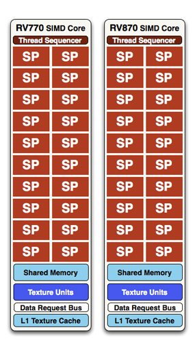
At a high level, the RV770 and Cypress SIMDs look very similar
The texture units located here have also been reworked. The first of these changes are that they can now read compressed AA color buffers, to better make use of the bandwidth they have. The second change to the texture units is to improve their interpolation speed by not doing interpolation. Interpolation has been moved to the SPs (this is part of DX11’s new Pull Model) which is much faster than having the texture unit do the job. The result is that a texture unit Cypress has a greater effective fillrate than one under RV770, and this will show up under synthetic tests in particular where the load-it and forget-it nature of the tests left RV770 interpolation bound. AMD’s specifications call for 68 billion bilinear filtered texels per second, a product of the improved texture units and the improved bandwidth to them.
Finally, if we move up another level, here is where we see the cause of the majority of Cypress’s performance advantage over RV770. AMD has doubled the number of SIMDs, moving from 10 to 20. This means twice the number of SPs and twice the number of texture units; in fact just about every statistic that has doubled between RV770 and Cypress is a result of doubling the SIMDs. It’s simple in concept, but as the SIMDs contain the most important units, it’s quite effective in boosting performance.
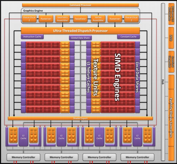
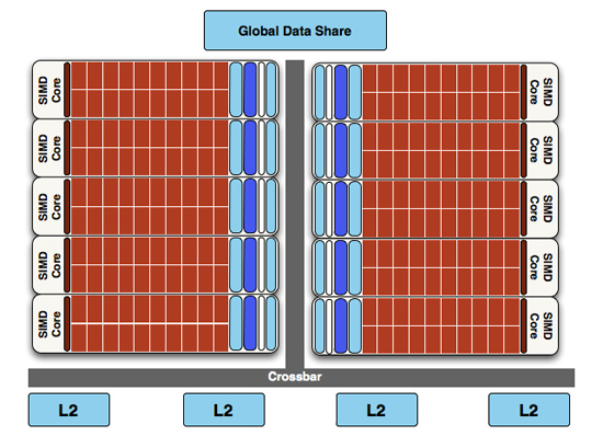
However with twice as many SIMDs, there comes a need to feed these additional SIMDs, and to do something with their products. To achieve this, the 4 L2 caches have been doubled from 64KB to 128KB. These large L2 caches can now feed data to L1 caches at 435GB/sec, up from 384GB/sec in RV770. Along with this the global data share has been quadrupled to 64KB.
RV770 vs...
Cypress
Next up, the ROPs have been doubled in order to meet the needs of processing data from all of those SIMDs. This brings Cypress to 32 ROPs. The ROPs themselves have also been slightly enhanced to improve their performance; they can now perform fast color clears, as it turns out some games were doing this hundreds of times between frames. They are also responsible for handling some aspects of AMD’s re-introduced Supersampling Anti-Aliasing mode, which we will get to later.
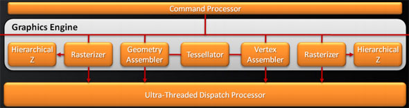
Last, but certainly not least, we have the changes to what AMD calls the “graphics engine”, primarily to bring it into compliance with DX11. RV770’s greatly underutilized tessellator has been upgraded to full DX11 compliance, giving it Hull Shader and Domain Shader capabilities, along with using a newer algorithm to reduce tessellation artifacts. A second rasterizer has also been added, ostensibly to feed the beast that is the 20 SIMDs.


327 Comments
View All Comments
BoFox - Friday, November 6, 2009 - link
Yep, that's turning up LOD to -1 or -2 depending on which game. It was done in Crysis, and with LOD at -2, it looked sharp with SSAA.The Wasrad - Wednesday, September 23, 2009 - link
Why are you using 4 gigs of ram with a 920?Do you understand how DDR3 memory works?
Ryan Smith - Wednesday, September 23, 2009 - link
Error when writing the chart. It has been corrected.Sc4freak - Wednesday, September 23, 2009 - link
Do you? The fact that the i7 920 works best in a triple-channel configuration has nothing to do with the fact that it uses DDR3.chizow - Wednesday, September 23, 2009 - link
Agreed and to add to that, the fact the third channel means very little when it comes to actual gaming performance makes it even less signficant. As compared to Lynnfield clock for clock, which is only dual channel:http://www.anandtech.com/cpuchipsets/showdoc.aspx?...">http://www.anandtech.com/cpuchipsets/showdoc.aspx?...
Von Matrices - Wednesday, September 23, 2009 - link
Could someone enlighten me as to why the 4870 X2 could be faster than the 5870 in some situations? It was noted it the article but never really explained. They have the same number of SP's, and one would expect crossfire scaling to be detrimental to the 4870 X2"s performance. Would this be indicative of the 5870 being starved for memory bandwidth in these situations or something else?Dobs - Wednesday, September 23, 2009 - link
4870x2 has 2Gb of DDR55870 only has 1 until the 2Gb edition comes out :)
nafhan - Wednesday, September 23, 2009 - link
Doesn't using dual GPU's effectively halve the onboard memory, as significant portions of the textures, etc. need to be duplicated? So, the 4870x2 has a memory disadvantage by requiring 2x memory to accomplish the same thing.chizow - Wednesday, September 23, 2009 - link
Right, with an X2 each GPU has a copy of the same frame buffer, so the total memory onboard is effectively halved. A 2GB frame buffer with 2 GPU is two of the same 1GB frame buffer mirrored on each.With the 5870 essentially being 2xRV790 on one chip, in order to accomplish the same frame rates on the same sized 1GB frame buffer, you would expect to need additional bandwidth to facilitate the transfers to and from the frame buffer and GPU.
chizow - Wednesday, September 23, 2009 - link
Ya he mentions bandwidth being a potential issue preventing the 5870 from mirroring the 4870X2's results.It could also be that the 5870's scheduler/dispatch processor aren't as efficient at extracting performance as driver forced AFR. Seems pretty incredible, seeing as physically doubling GPU transistors on a single die has always been traditionally better than multi-GPU scaling.
Similarly, it could be a CPU limitation where CF/SLI benefit more from multi-threaded driver performance, whereas a single GPU would be limited to a single fast thread or core's performance. We saw this a bit as well last year with the GT200s compared to G92s in SLI.