NVIDIA's Fermi: Architected for Tesla, 3 Billion Transistors in 2010
by Anand Lal Shimpi on September 30, 2009 12:00 AM EST- Posted in
- GPUs
Architecting Fermi: More Than 2x GT200
NVIDIA keeps referring to Fermi as a brand new architecture, while calling GT200 (and RV870) bigger versions of their predecessors with a few added features. Marginalizing the efforts required to build any multi-billion transistor chip is just silly, to an extent all of these GPUs have been significantly redesigned.
At a high level, Fermi doesn't look much different than a bigger GT200. NVIDIA is committed to its scalar architecture for the foreseeable future. In fact, its one op per clock per core philosophy comes from a basic desire to execute single threaded programs as quickly as possible. Remember, these are compute and graphics chips. NVIDIA sees no benefit in building a 16-wide or 5-wide core as the basis of its architectures, although we may see a bit more flexibility at the core level in the future.
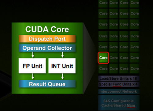
Despite the similarities, large parts of the architecture have evolved. The redesign happened at low as the core level. NVIDIA used to call these SPs (Streaming Processors), now they call them CUDA Cores, I’m going to call them cores.

All of the processing done at the core level is now to IEEE spec. That’s IEEE-754 2008 for floating point math (same as RV870/5870) and full 32-bit for integers. In the past 32-bit integer multiplies had to be emulated, the hardware could only do 24-bit integer muls. That silliness is now gone. Fused Multiply Add is also included. The goal was to avoid doing any cheesy tricks to implement math. Everything should be industry standards compliant and give you the results that you’d expect.
Double precision floating point (FP64) performance is improved tremendously. Peak 64-bit FP execution rate is now 1/2 of 32-bit FP, it used to be 1/8 (AMD's is 1/5). Wow.
NVIDIA isn’t disclosing clock speeds yet, so we don’t know exactly what that rate is yet.
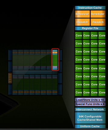
In G80 and GT200 NVIDIA grouped eight cores into what it called an SM. With Fermi, you get 32 cores per SM.

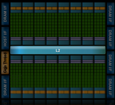
The high end single-GPU Fermi configuration will have 16 SMs. That’s fewer SMs than GT200, but more cores. 512 to be exact. Fermi has more than twice the core count of the GeForce GTX 285.
| Fermi | GT200 | G80 | |
| Cores | 512 | 240 | 128 |
| Memory Interface | 384-bit GDDR5 | 512-bit GDDR3 | 384-bit GDDR3 |
In addition to the cores, each SM has a Special Function Unit (SFU) used for transcendental math and interpolation. In GT200 this SFU had two pipelines, in Fermi it has four. While NVIDIA increased general math horsepower by 4x per SM, SFU resources only doubled.
The infamous missing MUL has been pulled out of the SFU, we shouldn’t have to quote peak single and dual-issue arithmetic rates any longer for NVIDIA GPUs.
NVIDIA organizes these SMs into TPCs, but the exact hierarchy isn’t being disclosed today. With the launch's Tesla focus we also don't know specific on ROPs, texture filtering or anything else related to 3D graphics. Boo.
A Real Cache Hierarchy
Each SM in GT200 had 16KB of shared memory that could be used by all of the cores. This wasn’t a cache, but rather software managed memory. The application would have to knowingly move data in and out of it. The benefit here is predictability, you always know if something is in shared memory because you put it there. The downside is it doesn’t work so well if the application isn’t very predictable.
Branch heavy applications and many of the general purpose compute applications that NVIDIA is going after need a real cache. So with Fermi at 40nm, NVIDIA gave them a real cache.
Attached to each SM is 64KB of configurable memory. It can be partitioned as 16KB/48KB or 48KB/16KB; one partition is shared memory, the other partition is an L1 cache. The 16KB minimum partition means that applications written for GT200 that require 16KB of shared memory will still work just fine on Fermi. If your app prefers shared memory, it gets 3x the space in Fermi. If your application could really benefit from a cache, Fermi now delivers that as well. GT200 did have an L1 texture cache (one per TPC), but the cache was mostly useless when the GPU ran in compute mode.

The entire chip shares a 768KB L2 cache. The result is a reduced penalty for doing an atomic memory op, Fermi is 5 - 20x faster here than GT200.


415 Comments
View All Comments
SiliconDoc - Wednesday, September 30, 2009 - link
No they did not post earnings, other than in the sense IN THE RED LOSSES called sales.shotage - Wednesday, September 30, 2009 - link
I'm not sure what your argument is SiliconDuck..But maybe you should stop typing and go into hybernation to await the GT300's holy ascension from heaven! FYI: It's unhealthy to have shrines dedicated to silicon dude. Get off the GPU cr@ck!!!
On a more serious note: Nvidia are good, ATI has gotten a lot better though.
I just bought a GTX260 recently, so I'm in no hurry to buy at the moment. I'll be eagerly awaiting to see what happens when Nvidia actually have the product launch and not just some lame paper/promo launch.
SiliconDoc - Wednesday, September 30, 2009 - link
My aregument is I've heard the EXACT SAME geekfoot whine before, twice in fact. Once for G80, once for GT200, and NOW, again....Here is what the guy said I responded to:
" Nvidia is painting itself into a corner in terms of engineering and direction. As a graphical engine, ATI's architecture is both smaller, cheaper to manufacture and scales better simply by combining chips or expanding # of units as mfg tech improves.. As a compute engine, Intel's Larabee will have unmatched parallel thread processing horsepower. What is Nvidia thinking trying to pass on this huge, monolithic albatross? It will lose on both fronts. "
---
MY ARGUMENT IS : A red raging rooster who just got their last two nvidia destruction calls WRONG for G80 and GT200 (the giant brute force non-profit expensive blah blah blah), are likely to the tune of 100% - TO BE GETTING THIS CRYING SPASM WRONG AS WELL.
---
When there is clear evidence Nvidia has been a markleting genius (it's called REBRANDING by the bashing red rooster crybabies) and has a billion bucks to burn a year on R&D, the argument HAS ALREADY BEEN MADE FOR ME.
-----
The person you should be questioning is the opinionated raging nvidia disser, who by all standards jives out an arrogant WHACK JOB on nvidia, declaring DUAL defeat...
QUOTETH ! "What is Nvidia thinking trying to pass on this huge, monolithic albatross? It will lose on both fronts. "
---
LOL that huge monolithic albatross COMMANDS $475,000.00 for 4 of them in some TESLA server for the collegiate geeks and freaks all over the world- I don't suppose there is " loss on that front" do you ?
ROFLMAO
Who are you questioning and WHY ? Why aren't you seeing clearly ? Did the reds already brainwash you ? Have the last two gigantic expensive cores "destroyed nvidia" as they predicted?
--
In closing "GET A CLUE".
shotage - Wednesday, September 30, 2009 - link
Found my clue.. I hope you get help in time: http://www.physorg.com/news171819640.html">http://www.physorg.com/news171819640.htmlSiliconDoc - Thursday, October 1, 2009 - link
You are your clue, and here is your buddy, your duplicate:" What is Nvidia thinking trying to pass on this huge, monolithic albatross? It will lose on both fronts."
Now, I quite understand denial is a favorite pasttime of losers, and you've effectively joined the red club. Let me convert for you.
" What is Ati thinking trying to pass on this over length, heat soaked, barely better afterthought? It will lose on it's only front."
-there you are schmucko, a fine example of real misbehavior you pass-
AaronJD - Wednesday, September 30, 2009 - link
While I definitely prefer the $200-$300 space that ATI released 48xx at, It seems like $400 is the magic number for single GPUs. Anything much higher than that is in multi-GPU space where you can get away with a higher price to performance ratio.If Nvidia can hit the market with well engineered $400 or so card that is easily pared down, then they can hit a market ATI would have trouble scaling to while being able to easily re-badge gimped silicon to meet whatever market segment they can best compete in with whatever quality yield they get.
Regarding Larabee, I think Nvidia's strategy is to just get in the door first. To compete against Intel's first offering they don't need to do something special, they just need to get the right feature set out there. If they can get developers writing for their hardware asap Tesla will have done its job.
Zingam - Thursday, October 1, 2009 - link
Until that thing from NVIDIA comes out AMD has time to work on a response and if they are not lazy or stupid they'll have a match for it.So in any way I believe that things are going to get more interesting than ever in the next 3 years!!!
:D ?an't wait to hear what DirectX 12 will be like!!!
My guess is that in 5 years we will have a truly new CPUs - that would do what GPUs + CPUs are doing together today.
Perhaps will come to the point where we'll get blade like home PCs. If you want more power you just shove in another board. Perhaps PC architecture will change completely once software gets ready for SMP.
chizow - Wednesday, September 30, 2009 - link
Nvidia is also launching Nexus at their GDC this week, a plug-in for Visual Studio that will basically integrate all of these various API under an industry standard IDE. That's the launching point imo for cGPU, Tesla and everything else Nvidia is hoping to accompolish outside of the 3D Gaming space with Fermi.Making their hardware more accessible to create those next killer apps is what's been missing in the past with GPGPU and CUDA. Now it'll all be cGPU and transparent in your workflow within Visual Studio.
As for the news of Fermi as a gaming GPU, very excited on that front, but not all that surprised really. Nvidia was due for another home run and it looks like Fermi might just clear the ball park completely. Tough times ahead for AMD, but at least they'll be able to enjoy the 5850/5870 success for a few months.
ilkhan - Wednesday, September 30, 2009 - link
If it plays games faster/prettier at the same or better price, who cares what the architecture looks like?On a similar note, if the die looks like that first image (which is likely) chopping it to smaller price points looks incredibly easy.
papapapapapapapababy - Wednesday, September 30, 2009 - link
"Architecturally, there aren't huge lessons to be learned from RV770"SNIF SNIF BS!
"ATI's approach is much more cautious"
more like "ATI's approach is much more FOCUSED"
( eyes on the ball people)
"While Fermi will play games, it is designed to be a general purpose compute machine."
nvidia, is starting to sound like Sony " the ps3 is not a console its a supercomputer @ HD movie player, it only does everything" guess what? people wanted to play games, nintendo ( the focused company, did that > games, not movies, not hd graphics, games, motion control) Sony - like nvidia here- didn't have the eyes on the ball.