NVIDIA's Fermi: Architected for Tesla, 3 Billion Transistors in 2010
by Anand Lal Shimpi on September 30, 2009 12:00 AM EST- Posted in
- GPUs
Architecting Fermi: More Than 2x GT200
NVIDIA keeps referring to Fermi as a brand new architecture, while calling GT200 (and RV870) bigger versions of their predecessors with a few added features. Marginalizing the efforts required to build any multi-billion transistor chip is just silly, to an extent all of these GPUs have been significantly redesigned.
At a high level, Fermi doesn't look much different than a bigger GT200. NVIDIA is committed to its scalar architecture for the foreseeable future. In fact, its one op per clock per core philosophy comes from a basic desire to execute single threaded programs as quickly as possible. Remember, these are compute and graphics chips. NVIDIA sees no benefit in building a 16-wide or 5-wide core as the basis of its architectures, although we may see a bit more flexibility at the core level in the future.
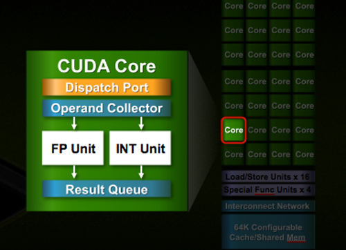
Despite the similarities, large parts of the architecture have evolved. The redesign happened at low as the core level. NVIDIA used to call these SPs (Streaming Processors), now they call them CUDA Cores, I’m going to call them cores.

All of the processing done at the core level is now to IEEE spec. That’s IEEE-754 2008 for floating point math (same as RV870/5870) and full 32-bit for integers. In the past 32-bit integer multiplies had to be emulated, the hardware could only do 24-bit integer muls. That silliness is now gone. Fused Multiply Add is also included. The goal was to avoid doing any cheesy tricks to implement math. Everything should be industry standards compliant and give you the results that you’d expect.
Double precision floating point (FP64) performance is improved tremendously. Peak 64-bit FP execution rate is now 1/2 of 32-bit FP, it used to be 1/8 (AMD's is 1/5). Wow.
NVIDIA isn’t disclosing clock speeds yet, so we don’t know exactly what that rate is yet.
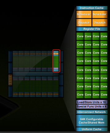
In G80 and GT200 NVIDIA grouped eight cores into what it called an SM. With Fermi, you get 32 cores per SM.

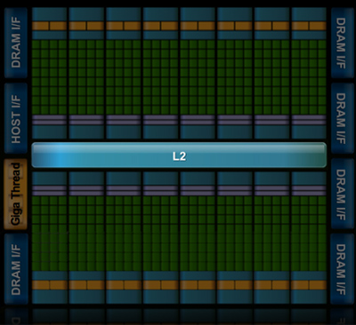
The high end single-GPU Fermi configuration will have 16 SMs. That’s fewer SMs than GT200, but more cores. 512 to be exact. Fermi has more than twice the core count of the GeForce GTX 285.
| Fermi | GT200 | G80 | |
| Cores | 512 | 240 | 128 |
| Memory Interface | 384-bit GDDR5 | 512-bit GDDR3 | 384-bit GDDR3 |
In addition to the cores, each SM has a Special Function Unit (SFU) used for transcendental math and interpolation. In GT200 this SFU had two pipelines, in Fermi it has four. While NVIDIA increased general math horsepower by 4x per SM, SFU resources only doubled.
The infamous missing MUL has been pulled out of the SFU, we shouldn’t have to quote peak single and dual-issue arithmetic rates any longer for NVIDIA GPUs.
NVIDIA organizes these SMs into TPCs, but the exact hierarchy isn’t being disclosed today. With the launch's Tesla focus we also don't know specific on ROPs, texture filtering or anything else related to 3D graphics. Boo.
A Real Cache Hierarchy
Each SM in GT200 had 16KB of shared memory that could be used by all of the cores. This wasn’t a cache, but rather software managed memory. The application would have to knowingly move data in and out of it. The benefit here is predictability, you always know if something is in shared memory because you put it there. The downside is it doesn’t work so well if the application isn’t very predictable.
Branch heavy applications and many of the general purpose compute applications that NVIDIA is going after need a real cache. So with Fermi at 40nm, NVIDIA gave them a real cache.
Attached to each SM is 64KB of configurable memory. It can be partitioned as 16KB/48KB or 48KB/16KB; one partition is shared memory, the other partition is an L1 cache. The 16KB minimum partition means that applications written for GT200 that require 16KB of shared memory will still work just fine on Fermi. If your app prefers shared memory, it gets 3x the space in Fermi. If your application could really benefit from a cache, Fermi now delivers that as well. GT200 did have an L1 texture cache (one per TPC), but the cache was mostly useless when the GPU ran in compute mode.

The entire chip shares a 768KB L2 cache. The result is a reduced penalty for doing an atomic memory op, Fermi is 5 - 20x faster here than GT200.


415 Comments
View All Comments
Zingam - Thursday, October 1, 2009 - link
No no! This is just on paper! When will see it for real!! Oh... Q2-3-4 next year! :)So you cannot claim they have the better thing because they don't have it yet! And don't forget next year we might have the head-smashing Larrabee!
:)
Who knows!!! I think you are way to biased and not objective when you type!
chizow - Thursday, October 1, 2009 - link
Heheh if Q2 is what you want to believe when you cry yourself to sleep every night, so be it. ;)Seriously though, its looking like late Q4 or early Q1 and its undoubtedly meant for one single purpose: to destroy the world of ATI GPUs.
As for Larrabee lol...check out some of the IDF news about it. Even Anand hints at Laughabee's failure in his article here. It may compete as a GPGPU extension of x86, but not as a traditional 3D raster, not even close.
SiliconDoc - Thursday, October 1, 2009 - link
Gosh you'd be correct except here is the FERMIhttp://www.fudzilla.com/content/view/15762/1/">http://www.fudzilla.com/content/view/15762/1/
There it is bubba. you blew your yap wide open in ignorance and LOST.
Good job, you've got plenty of company.
ClownPuncher - Thursday, October 1, 2009 - link
Wow, a video card! On top of that pcb could be a cat shit for all we know. The card does not exist, because I can't touch it, I can't buy it, and I can't play games on it.Also, the fact that you seem to get all of your info from Fudzilla speaks volumes. All of your syphillus induced mad ramblings are tiresome.
Lifted - Thursday, October 1, 2009 - link
I see what appears to be a PCB with some plastic attached, and possibly a fan in there as well. Yawn.ksherman - Wednesday, September 30, 2009 - link
Really like these kind of leaps in computing power, I find it fascinating. A shame that it seems nVidia is pulling a bit away from the mainstream graphics segment, but I suppose that means that the new cards from ATI/AMD are the undisputed choice for a graphics card in the next few months. 5850 it is!fri2219 - Wednesday, September 30, 2009 - link
For the love of Strunk and White, stop murdering English in that manner- it detracts from the text buried between banner ads.Sunday Ironfoot - Wednesday, September 30, 2009 - link
nVidia have invented a new way to fry eggs, just crack one open on top of their GPU and play some Crysis. :-)SiliconDoc - Wednesday, September 30, 2009 - link
Let's crack it on page 4. A mjore efficient architecture max threads in flight. Although the DOWNSIDE is sure to be mentioned FIRST as in "not as many as GT200", and the differences mentioned later, the hidden conclusion with the dissing included is apparent.Let's draw it OUT.
---
What should have been said 1st:
Nvidia's new core is 4 times more efficient with threads in flight, so it reduces the number of those from 30,720 to 24,576, maintaining an impressive INCREASE.
---
Yes, now the simple calculation:
GT200 30720x2 = 61,440 GT300 24576x4 = 98,304
at the bottom we find second to last line the TRUTH, before the SLAM on the gt200 ends the page:
" After two clocks, the dispatchers are free to send another pair of half-warps out again. As I mentioned before, in GT200/G80 the entire SM was tied up for a full 8 cycles after an SFU issue."
4 to 1, 4 times better, 1/4th the clock cycles needed
" The flexibility is nice, or rather, the inflexibility of GT200/G80 was horrible for efficiency and Fermi fixes that. "
LOL
With a 4x increase in this core design area, first we're told GT200 "had more" then were told Fermi is faster in terms that allow > the final tale, GT200 sucks.
--
I just LOVE IT, I bet nvidia does as well.
tamalero - Thursday, October 1, 2009 - link
on paper everything looks amazing, just like the R600 did in its time, and the Nvidia FX series as well. so please, just shut up and start spreading your FUD until theres real information, real benches, real useful stuff.